- 您现在的位置:买卖IC网 > Sheet目录2006 > LTC2418IGN#TRPBF (Linear Technology)IC ADC 24BIT DIFF INPUT 28SSOP
LTC2414/LTC2418
15
241418fa
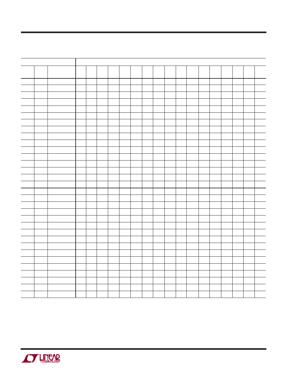
Table 2. Channel Selection for the LTC2418
MUX ADDRESS
CHANNEL SELECTION
ODD/
SGL
SIGN
A2 A1 A0
0
123456789
10
11
12
13
14
15
COM
*
000
0
IN+
IN–
000
0
1
IN+
IN–
000
1
0
IN+
IN–
000
1
IN+
IN–
001
0
IN+
IN–
001
0
1
IN+
IN–
001
1
0
IN+
IN–
001
1
IN+
IN–
010
0
IN–
IN+
010
0
1
IN–
IN+
010
1
0
IN–
IN+
010
1
IN–
IN+
011
0
IN–
IN+
011
0
1
IN–
IN+
011
1
0
IN–
IN+
011
1
IN–
IN+
100
0
IN+
IN–
100
0
1
IN+
IN–
100
1
0
IN+
IN–
100
1
IN+
IN–
101
0
IN+
IN–
101
0
1
IN+
IN–
101
1
0
IN+
IN–
101
1
IN+
IN–
110
0
IN+
IN–
110
0
1
IN+
IN–
110
1
0
IN+
IN–
110
1
IN+
IN–
111
0
IN+
IN–
111
0
1
IN+
IN–
111
1
0
IN+
IN–
111
1
IN+
IN–
*Default at power up
APPLICATIO S I FOR ATIO
WU
UU
Output Data Format
The LTC2414/LTC2418 serial output data stream is 32 bits
long. The first 3 bits represent status information indicat-
ing the sign and conversion state. The next 23 bits are the
conversion result, MSB first. The next 5 bits (Bit 5 to Bit 1)
indicate which channel the conversion just performed was
selected. The address bits programmed during this data
output phase select the input channel for the next conver-
sion cycle. These address bits are output during the sub-
sequent data read, as shown in Figure 3b. The last bit is a
发布紧急采购,3分钟左右您将得到回复。
相关PDF资料
LTC2431IMS#TRPBF
IC ADC 20BIT DIFFINPUT/REF10MSOP
LTC2433-1IMS#TRPBF
IC ADC DIFF 16BIT 3WIRE 10-MSOP
LTC2435CGN#TRPBF
IC ADC DIFF I/REF 20BIT 16-SSOP
LTC2442IG#PBF
IC ADC 24BIT 4CH 36-SSOP
LTC2446IUHF#TRPBF
IC ADC 24BIT 8CH HI SPEED 38QFN
LTC2448IUHF#TRPBF
IC ADC 24BIT HI SPEED 38QFN
LTC2451ITS8#TRPBF
IC ADC 16BIT DELTA SIG TSOT23-8
LTC2452ITS8#TRPBF
IC ADC 16BIT DELTA SIG TSOT23-8
相关代理商/技术参数
LTC2420CS8
功能描述:IC ADC 20BIT MICRPWR W/OSC 8SOIC RoHS:否 类别:集成电路 (IC) >> 数据采集 - 模数转换器 系列:- 标准包装:1,000 系列:- 位数:16 采样率(每秒):45k 数据接口:串行 转换器数目:2 功率耗散(最大):315mW 电压电源:模拟和数字 工作温度:0°C ~ 70°C 安装类型:表面贴装 封装/外壳:28-SOIC(0.295",7.50mm 宽) 供应商设备封装:28-SOIC W 包装:带卷 (TR) 输入数目和类型:2 个单端,单极
LTC2420CS8#PBF
功能描述:IC ADC 20BIT MICRPWR W/OSC 8SOIC RoHS:是 类别:集成电路 (IC) >> 数据采集 - 模数转换器 系列:- 标准包装:1 系列:microPOWER™ 位数:8 采样率(每秒):1M 数据接口:串行,SPI? 转换器数目:1 功率耗散(最大):- 电压电源:模拟和数字 工作温度:-40°C ~ 125°C 安装类型:表面贴装 封装/外壳:24-VFQFN 裸露焊盘 供应商设备封装:24-VQFN 裸露焊盘(4x4) 包装:Digi-Reel® 输入数目和类型:8 个单端,单极 产品目录页面:892 (CN2011-ZH PDF) 其它名称:296-25851-6
LTC2420CS8#PBF
制造商:Linear Technology 功能描述:A/D Converter (A-D) IC
LTC2420CS8#TR
功能描述:IC A/D CONV 20BIT MICRPWR 8-SOIC RoHS:否 类别:集成电路 (IC) >> 数据采集 - 模数转换器 系列:- 标准包装:1,000 系列:- 位数:16 采样率(每秒):45k 数据接口:串行 转换器数目:2 功率耗散(最大):315mW 电压电源:模拟和数字 工作温度:0°C ~ 70°C 安装类型:表面贴装 封装/外壳:28-SOIC(0.295",7.50mm 宽) 供应商设备封装:28-SOIC W 包装:带卷 (TR) 输入数目和类型:2 个单端,单极
LTC2420CS8#TRPBF
功能描述:IC ADC 20BIT MICRPWR W/OSC 8SOIC RoHS:否 类别:集成电路 (IC) >> 数据采集 - 模数转换器 系列:- 标准包装:1,000 系列:- 位数:16 采样率(每秒):45k 数据接口:串行 转换器数目:2 功率耗散(最大):315mW 电压电源:模拟和数字 工作温度:0°C ~ 70°C 安装类型:表面贴装 封装/外壳:28-SOIC(0.295",7.50mm 宽) 供应商设备封装:28-SOIC W 包装:带卷 (TR) 输入数目和类型:2 个单端,单极
LTC2420CS8PBF
制造商:Linear Technology 功能描述:ADC,LTC2420C 20bit D-S SPI SOIC
LTC2420IS8
功能描述:IC ADC 20BIT MICROPOWER 8SOIC RoHS:否 类别:集成电路 (IC) >> 数据采集 - 模数转换器 系列:- 标准包装:1,000 系列:- 位数:16 采样率(每秒):45k 数据接口:串行 转换器数目:2 功率耗散(最大):315mW 电压电源:模拟和数字 工作温度:0°C ~ 70°C 安装类型:表面贴装 封装/外壳:28-SOIC(0.295",7.50mm 宽) 供应商设备封装:28-SOIC W 包装:带卷 (TR) 输入数目和类型:2 个单端,单极
LTC2420IS8#PBF
功能描述:IC ADC 20BIT MICRPWR W/OSC 8SOIC RoHS:是 类别:集成电路 (IC) >> 数据采集 - 模数转换器 系列:- 标准包装:1 系列:microPOWER™ 位数:8 采样率(每秒):1M 数据接口:串行,SPI? 转换器数目:1 功率耗散(最大):- 电压电源:模拟和数字 工作温度:-40°C ~ 125°C 安装类型:表面贴装 封装/外壳:24-VFQFN 裸露焊盘 供应商设备封装:24-VQFN 裸露焊盘(4x4) 包装:Digi-Reel® 输入数目和类型:8 个单端,单极 产品目录页面:892 (CN2011-ZH PDF) 其它名称:296-25851-6